PCB prototyping is a vital stage in this process, enabling designers and engineers to validate their ideas pcb prototyping and development, test functionality, and refine their designs before moving to mass production. This guide provides a comprehensive overview of PCB prototyping and development, offering essential insights and practical tips to ensure a successful transition from idea to prototype.
Understanding PCB Prototyping
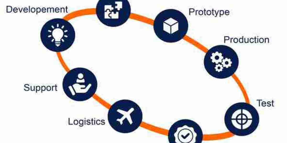
PCB prototyping involves creating a preliminary version of a circuit board to test and validate the design before full-scale production. This stage is crucial for identifying design flaws, verifying functionality, and ensuring that the final product meets all specifications. Prototyping allows designers to make necessary adjustments and improvements, ultimately leading to a more reliable and efficient final product.
Steps in PCB Prototyping and Development
1. Conceptualization and Design
The first step in PCB development is to convert your idea into a detailed design. This phase involves:
Defining Specifications: Clearly outline the technical requirements, including functionality, dimensions, and performance criteria.
Schematic Design: Create a schematic diagram that represents the electrical connections and components of the PCB. This is the blueprint for the circuit board.
Component Selection: Choose the appropriate components based on your design requirements, such as resistors, capacitors, ICs, and connectors.
2. PCB Layout Design
Once the schematic is complete, the next step is to design the PCB layout. This involves:
Creating the PCB Layout: Use PCB design software to translate the schematic into a physical layout. Arrange the components and route the electrical connections.
Design Rule Check (DRC): Perform a Design Rule Check to ensure that the layout adheres to manufacturing and electrical specifications.
Signal Integrity: Analyze the layout for signal integrity issues, such as crosstalk and electromagnetic interference.
3. Prototype Fabrication
With the design finalized, the next step is to fabricate the PCB prototype. This process includes:
PCB Manufacturing: Send the PCB design files to a fabrication service that will produce the physical PCB. This includes etching the copper layers, drilling holes, and applying solder masks.
Component Assembly: Once the PCB is fabricated, components are mounted onto the board. This can be done through surface-mount technology (SMT) or through-hole mounting.
4. Testing and Validation
After assembly, the PCB prototype undergoes rigorous testing to ensure it meets the design specifications. Key testing processes include:
Functional Testing: Verify that the PCB performs its intended functions correctly. This includes testing power, signal integrity, and overall performance.
Debugging: Identify and fix any issues or defects discovered during testing. This may involve modifying the design or replacing components.
Thermal Testing: Check for thermal issues by monitoring the temperature of the PCB under operational conditions.
5. Iteration and Refinement
Based on the test results, you may need to make revisions to the PCB design. This iterative process involves:
Design Modifications: Adjust the design to address any issues found during testing. This could include rerouting traces, changing component placements, or upgrading components.
Re-fabrication: Produce a new prototype incorporating the changes. This ensures that the revised design is tested and validated.
6. Preparing for Production
Once the prototype meets all requirements, prepare for mass production. This stage involves:
Final Design Review: Conduct a final review of the design and prototype to ensure everything is in order before scaling up production.
Manufacturing Documentation: Prepare detailed manufacturing documentation, including assembly instructions and quality control procedures.
Supplier Coordination: Work with manufacturing partners to set up production runs, ensuring that they have all necessary information and resources.
Best Practices in PCB Prototyping
1. Use Reliable Design Tools
Invest in high-quality PCB design software that offers robust features for schematic capture, layout design, and simulation. Popular tools include Altium Designer, Eagle PCB, and KiCad.
2. Focus on Design for Manufacturability (DFM)
Consider manufacturing constraints during the design phase. Ensure that your design adheres to standard practices for ease of fabrication and assembly, such as proper component spacing and trace width.
3. Communicate Clearly with Fabricators
Provide clear and detailed design files to your PCB fabricator. Include all necessary information such as layer stack-up, component placement, and solder mask details to avoid misunderstandings and errors.
4. Perform Thorough Testing
Conduct comprehensive testing of your PCB prototype to uncover potential issues early. Utilize both automated and manual testing methods to ensure thorough validation.
5. Document Changes and Iterations
Maintain detailed records of design changes and testing results. This documentation is invaluable for tracking progress, troubleshooting issues, and guiding future iterations.
Conclusion
pcb prototyping and development are essential steps in bringing an electronic product from concept to reality. By following a structured approach—from initial design through testing and refinement—you can ensure that your PCB prototype meets all functional and performance requirements. Emphasizing best practices and maintaining clear communication with your fabrication partners will further enhance the success of your PCB development process.
Follow Us More Links:-
Follow Us On Facebook:- https://www.facebook.com/synchronics
Follow Us On Instagram:- https://www.instagram.com/synchronicselectronics/
Follow Us On Linkedin:- https://in.linkedin.com/company/synchronics
Follow Us On Twitter:- https://x.com/synchronics
Add:- 4th Floor, Lotus Enora, Opp. Rutu Villa Bunglows, 24 Mt. Main Road, New Alkapuri, Gotri, Vadodara 390 021, Gujarat (INDIA)
Call Us :- +91-704-308-4455 || +91-704-309-4455 || +91-265-400-1555 || +91-265-356-1183
Email Us:- email@synchronics.co.in